Manufacturing Process
We recreate the extreme conditions of a dying star inside our cleanroom reactors. Discover how we grow perfect diamond lattice structures atom by atom, turning gas into the ultimate solid.
Seed Selection & Preparation
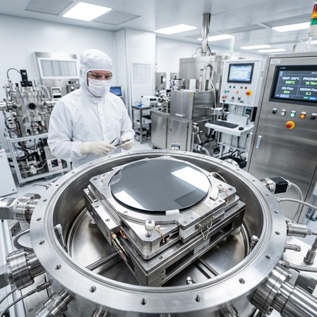
The foundation of a perfect diamond is a perfect seed. For polycrystalline growth, highly polished silicon or refractory metal wafers are meticulously cleaned and uniformly seeded with nanodiamond particles. For single-crystal growth, we utilize carefully selected, defect-free diamond plates. These substrates undergo rigorous chemical etching in our cleanrooms to remove any organic contaminants or native oxides, ensuring an immaculate atomic surface for the plasma to interact with.
Microwave Plasma CVD Growth
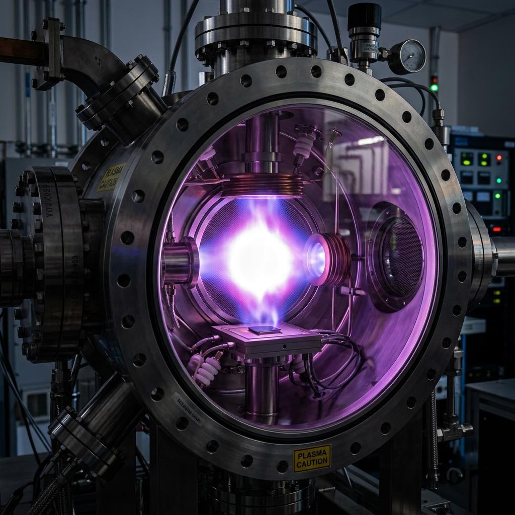
The prepared substrates are loaded into our proprietary microwave plasma reactors. The chamber is evacuated to an ultra-high vacuum before highly purified methane (the carbon source) and hydrogen gases are introduced. High-power microwaves ignite the gases into a brilliant, intensely hot plasma, frequently exceeding 3000°C. Hydrogen radicals continuously etch away weak non-diamond (sp2) carbon bonds, while carbon atoms deposit atom-by-atom (sp3 bonds) onto the substrate, growing the diamond lattice over several weeks.
Wafer Slicing & Laser Coring
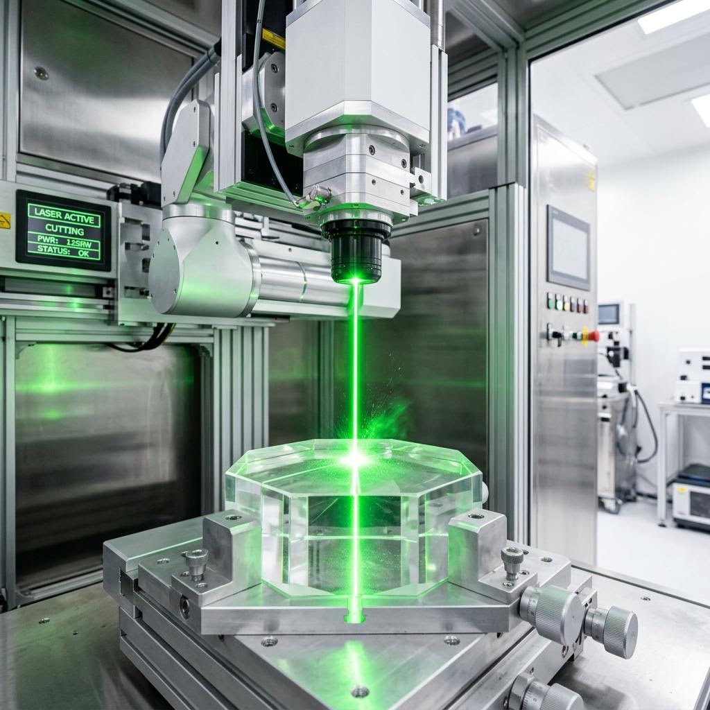
Because lab-grown diamond exhibits extreme hardness, traditional cutting tools are useless. Once the desired crystalline thickness is achieved, the raw diamond blocks or thick wafers are harvested. We deploy advanced, high-power nanosecond green lasers to precisely slice single-crystal blocks into thin plates or to core out specific wafer diameters from large polycrystalline discs. This non-contact laser ablation ensures zero mechanical stress is applied to the fragile crystal structure.
Precision Grinding & Shaping
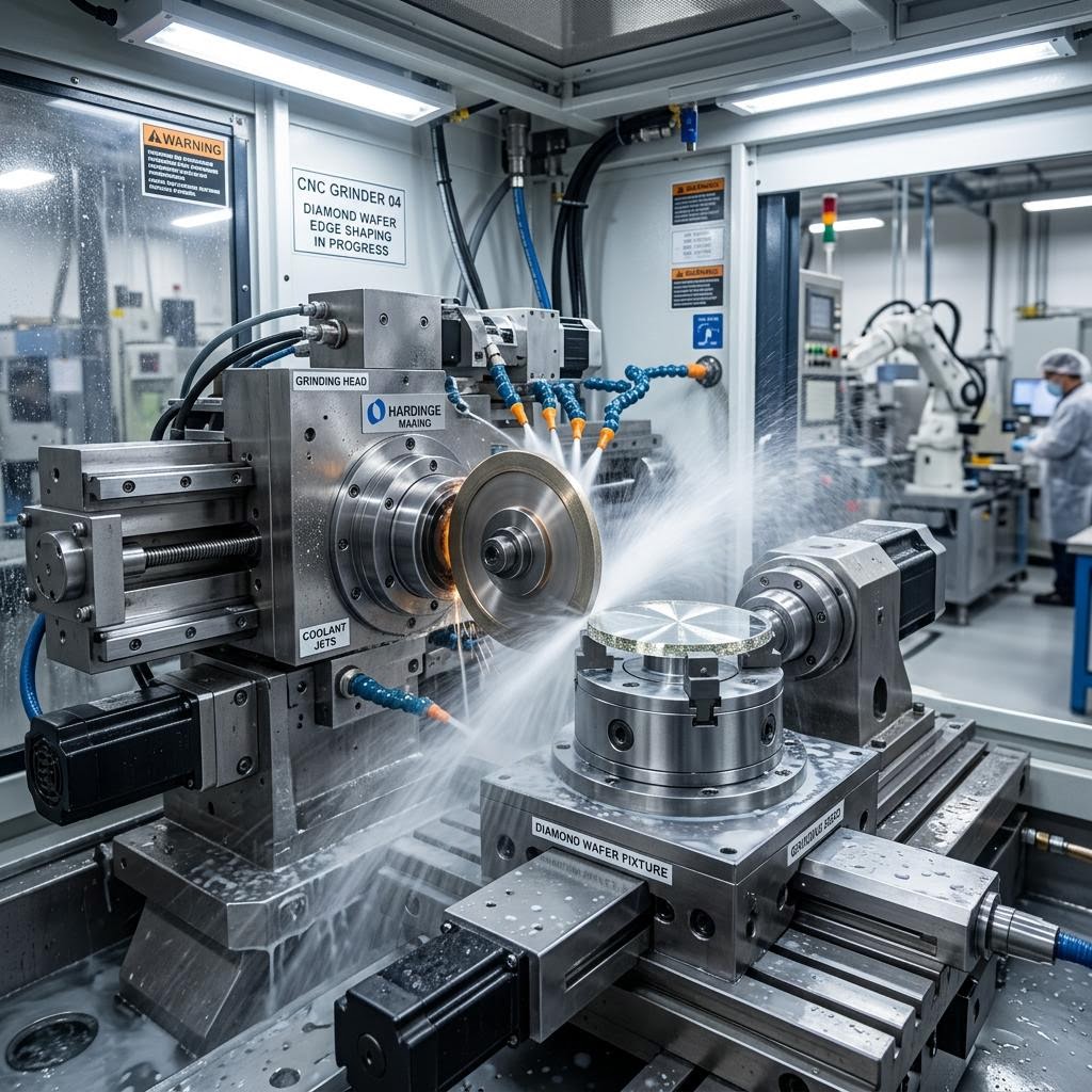
The raw laser-cut edges and top surfaces of the diamond material require aggressive planarization. Using specialized multi-axis CNC grinding machines equipped with resin-bonded diamond grit wheels, we aggressively grind the diamond down to the client's specified thickness and geometric tolerances. Water-cooling jets run continuously to manage friction heat, bringing the rough diamond down to a highly uniform, flat profile ready for final polish.
CMP Polishing
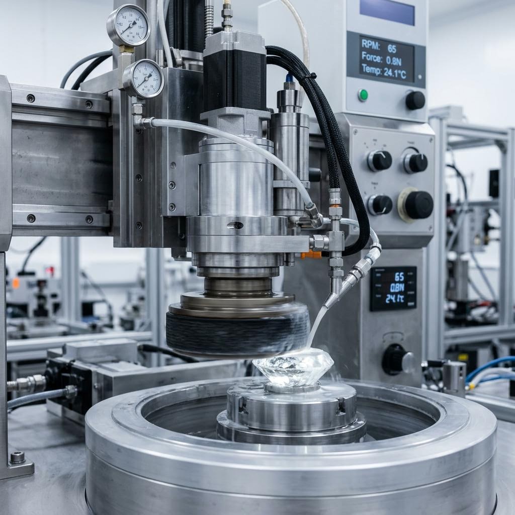
To achieve the extreme surface specifications required for semiconductor and optical applications, standard grinding is insufficient. The diamond substrates undergo Chemical-Mechanical Polishing (CMP). By combining a reactive chemical slurry with ultra-fine abrasive pads, we polish the diamond's surface down to sub-nanometer roughness (Ra < 5nm). This mirror-like finish is critical for ensuring perfect thermal contact in heat spreaders and zero light scattering in optical windows.
Final Inspection & Quality Control
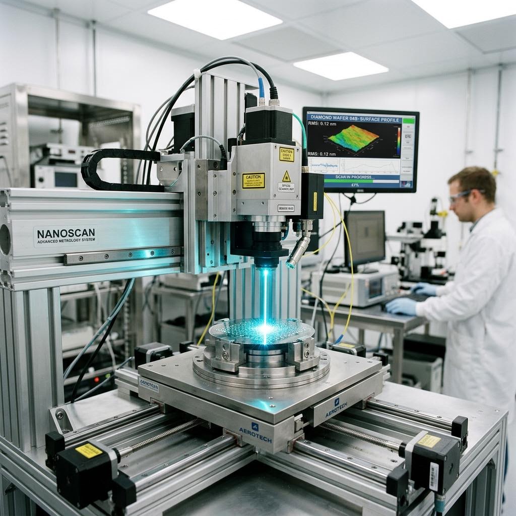
Every single wafer and plate is subjected to uncompromising metrology before it leaves our facility. We utilize Raman spectroscopy to verify 100% sp3 carbon bonding, X-ray diffraction to confirm crystalline perfection, and laser flash analysis to certify exact thermal conductivity ratings. Only when a substrate meets the precise dimensional, thermal, and optical tolerances of the engineering brief is it certified and packaged in our ISO Class 4 cleanroom.